|
CRYSCORE OPTOELECTRONIC LIMITED
|
PLANE (1-102) SAPPHIRE WAFERS
| Price: | 10.0 USD |
| Payment Terms: | T/T |
| Place of Origin: | Henan, China (Mainland) |
|
|
|
| Add to My Favorites | |
| HiSupplier Escrow |
Product Detail
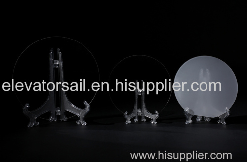
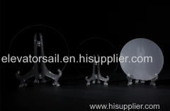
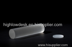
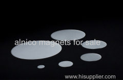
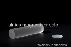
R plane(1-102) sapphire wafers are preferred for the hetero-epitaxial deposition of silicon used in microelectronic IC applications.
R plane(1-102) sapphire wafers are preferred for the hetero-epitaxial deposition of silicon used in microelectronic IC applications. R plane is the non-polar plane of sapphire. So the different positions of R-plane in sapphire devices, the mechanical, thermal, electrical and optical properties of sapphire devices will vary greatly, which will also affect the subsequent processing performance, processing efficiency and processing yield of sapphire devices.
In order to make the crystal structure of sapphire ingot and subsequent sapphire products consistent, the more common method is to process an A-direction surface on the sapphire ingot as the flat orientation of sapphire wafer (subsequent sapphire products), so that the R-direction position of sapphire ingot and the wafer is consistent.
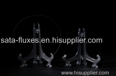
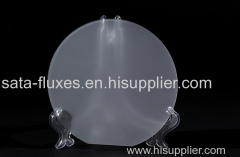
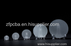
Specifications of R-Plane (1-102) Sapphire Wafers
Item | 2 -inch R-plane(1-102) 430μm Sapphire Wafers | |
Crystal Materials | 99,999%, High Purity, Monocrystalline Al2O3 | |
Grade | Prime, Epi-Ready | |
Surface Orientation | R-plane(1-102) | |
Diameter | 50.8 mm +/- 0.1 mm | |
Thickness | 430 μm +/- 25 μm | |
Primary Flat Orientation | 45 +/- 1deg. counter-clockwise from C-axis projection on R-plane | |
Primary Flat Length | 16.0 mm +/- 1.0 mm | |
Single Side Polished | Front Surface | Epi-polished, Ra < 0.5 nm (by AFM) |
(SSP) | Back Surface | Fine ground, Ra = 0.8 μm to 1.2 μm |
Double Side Polished | Front Surface | Epi-polished, Ra < 0.5 nm (by AFM) |
(DSP) | Back Surface | Epi-polished, Ra < 0.5 nm (by AFM) |
TTV | < 10 μm | |
BOW | < 10 μm | |
WARP | < 10 μm | |
Cleaning / Packaging | Class 100 cleanroom cleaning and vacuum packaging, | |
25 pieces in one cassette packaging or single piece packaging. | ||
Note: Custom sapphire wafers with any orientation and any thickness can be provided.
We have sapphire substrates,r plane sapphire and Sapphire Windows,RFQ today.

