|
CRYSCORE OPTOELECTRONIC LIMITED
|
PATTERNED SAPPHIRE SUBSTRATES PATTERNED SAPPHIRE SUBSTRATES
| Place of Origin: | Henan, China (Mainland) |
|
|
|
| Add to My Favorites | |
| HiSupplier Escrow |
Product Detail
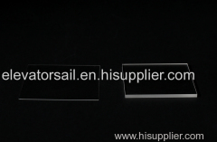
patterned sapphire substrates
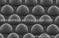
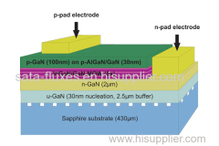
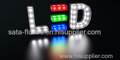
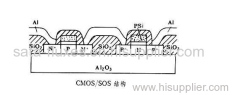
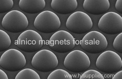
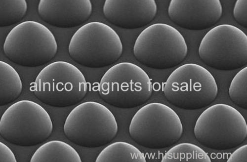
Sapphire wafer is the most widely used substrate material in semiconductor lighting industry, and patterned sapphire substrate (PSS) is the general method to improve the luminous efficiency of semiconductor lighting devices. These sapphire substrates are with periodic structures of various shapes such as cone, dome, pyramid, and pillar, etc.
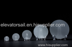
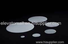
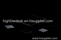
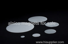
Different Sizes of Patterned Sapphire Substrates
2-Inch
2 Inch Patterned Sapphire Substrates
PSS is to design and manufacture specific nano-scale microstructure pattern on sapphire substrate.
4-Inch
4 Inch Patterned Sapphire Substrates
Patterned Sapphire Substrates (PSS) is micro-patterned sapphire substrate used to for GaN based light emitting diodes(LEDS).
CRYSCORE OPTOELECTRONIC LIMITED has been a professional manufacturer, we provide sapphire optics, pss wafer, pss sapphire, Patterned sapphire substrate and etc. Want to know more? Please contact us.
Related Search
Find more related products in following catalogs on Hisupplier.com
Company Info
CRYSCORE OPTOELECTRONIC LIMITED [China (Mainland)]
Business Type:Manufacturer
City: Jiaozuo
Province/State: Henan
Country/Region: China (Mainland)